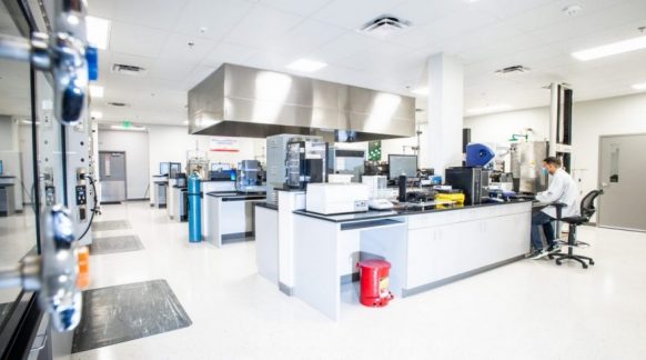
Machining Materials for Multilayer Circuits
Electronic products continue to add functions in smaller packages, even for traditionally large systems such as computer servers and wired telecommunications networks. Multilayer circuits are essential for providing more electronic capabilities in smaller sizes, often relying on highly integrated circuits (ICs) and surface-mount-technology components to fit all the functions. Reliable multilayer printed circuit boards (PCBs) require thoughtful selection of materials for each conductive layer and its insulating layers. As important, the machining and processing of those circuit materials determines the quality of a single-layer, double-sided, or multilayer PCB or even a hybrid PCB formed of two or more different circuit boards.
Circuit machining equipment has grown in sophistication. While mechanical drills are commonly used to form alignment holes and thruholes between circuit layers, laser drilling equipment provides precision machining without physical wear on drill bits. High-resolution, precision machining in combination with advanced photoresist systems are needed to form the shrinking dimensions of circuit geometries required for higher-speed digital (HSD) circuits, wireless networks, and applications at RF/microwave (MW) frequencies, especially for densely packed multilayer circuits with growing numbers of features and functions. As important as the precision of the circuit machining equipment is the availability of “process-friendly” circuit materials that lend themselves to strong lamination adherence, clean thruhole formation, and fabrication of the exact linewidths and spacings needed to support HSD and high-frequency RF/MW circuits.
Fitting Formulas
Modern requirements for multiple functions in small electronic products, such as smartphones or wearable medical devices, down-sized high-data-rate boards, or even miniaturized telecommunications boards, may no longer be increasing the layer counts of multilayer circuits but they are increasing the complexity of the processes required to fabricate the circuit boards. Working with circuit materials that must be processed with advanced techniques requires circuit fabrication facilities to maintain sophisticated equipment, such as laser drills, and personnel with the skills to use the equipment. Using circuit materials that are not “process friendly” requires additional time and processing steps compared to many of the materials offered by the Isola Group (www.isola-group.com), which have been engineered for ease of use.
Materials that require complex machining and processing can add to the total time and cost taken to form a complete multilayer circuit or high-density-interconnect (HDI) assembly. The number of layers refers to the conductive layers, which provide interconnections between ICs and other components. The conductive layers serve as planes for different functions, such as signal, ground, and power planes, with prepreg materials providing insulation and isolation between conductive layers. The placement and spacing of the conductive layers are parts of the design and layout of any multilayer circuit or HDI assembly, with good signal-to-ground connections, for example, resulting in good electromagnetic-compatibility (EMC) and electromagnetic-interference (EMI) performance.
Material quality, such as the smoothness of the copper foils used as conductive layers and the stability of the dielectric constant (Dk) for circuit laminate and prepreg materials, contributes a great deal to the performance levels possible with a given HDI assembly. But PCB fabrication and machining are also essential to extracting optimum performance levels from a set of circuit materials. And building PCBs and HDIs with materials that not only are well suited but engineered for modern fabrication processes can result in actual circuit performance that is as close as possible to the levels promised by computer circuit simulations.
The HDI buildup board starts with a double-sided core, with a layer-by-layer buildup by lamination with prepregs. The compatibility of the materials is important for reliability and electrical performance. For cost-effectiveness, for example, FR-4 circuit boards provide suitable stability and performance for power and ground planes as well as for lower-speed digital and lower-frequency RF signal planes. Higher-speed, higher-frequency signal planes require materials with higher electrical and mechanical (often environmental) stability than FR-4 circuit materials so that low-loss dielectric materials with low Dk and low dissipation factor (Df) have often supported the higher-speed, higher-frequency signal planes in HDIs, although some low-loss circuit materials require sophisticated processing methods for dependable, high-yield circuits. Since they are also combined with other circuit materials such as FR-4 in HDIs, interconnections between layers in these high-speed, high-frequency, multiple-material HDIs must be carefully formed for optimum impedance matching between signal and ground planes.
The Isola Group and its Asia Pacific division have worked closely with circuit designers and fabricators to understand specific requirements for multilayer circuits and HDIs with multiple materials, especially when they must be machined for HSD and RF/MW circuits. As an example, Astra® MT77 laminates and prepregs are usable for RF/MW circuits through W-band frequencies. Laminates are available with copper weights from 0.5 to 2.0 oz. (with custom foils available on request) and can be used with prepregs for multilayer circuits and HDIs with any number of layers.
Astra®MT77 circuit materials feature good flow to fill and FR-4 process compatibility to simplify multilayer circuit production. These circuit materials offer a cost-effective alternative to PTFE circuit materials without the machining complexity of PTFE or PTFE’s special thruhole treatments. They exhibit a low dielectric constant (Dk) of 3.00 with consistent performance to 100 GHz. The Dk for each production lot is controlled and measured from 2 to 10 GHz before shipping to customers. For good circuit stability with temperature, critical for automotive electronics applications, they maintain that Dk value from -40 to +125°C. They are compatible with lead-free, RoHS-compliant PCB manufacturing processes and are excellent circuit candidates for HDI assemblies and RF/MW antennas that can be machined easily and effectively.
14 December 2021


